
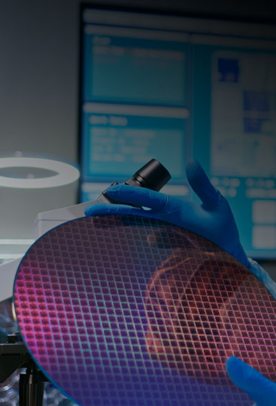

Integrated Optics
Photonic integrated circuits (PICs) are tiny yet powerful chips capable of doing awesome things! PICs can implement complex optical systems with an unparalleled level of miniaturization, performance, and cost efficiency compared to conventional optics.
However, no single chip can do it all! There are multiple technology platforms with varying levels of maturity competing in the market, each uniquely suited for developing specific functionalities. There is no one-size-fits-all when it comes to PICs. That’s where FAR PHOTONICS comes in to guide you through the turbulent waters of the PIC landscape and help you navigate the choices:
Material Platform
System-Level Design
Component-Level Design
Layout Generation
Generate layouts that meet or exceed the strict requirements of your application and foundry.
Foundry Liaison
And finally, liaise with the foundry to bring your PIC design to life!
Experimental Setups
Packaging & Assembly
FAR PHOTONICS has extensive experience in navigating the challenging waters of PIC packaging and assembly, and can guide you through the following crucial steps of your journey:

Materials Selection
Package Design
Thermal Design
Parts Inspection
Cleaning Procedures
Die Bonding Procedures
Wire Bonding Procedures
Sub-Micron Alignment and Attachment
Dispensing and Curing Protocols
Opto-Mechanics
The design requirements of a beam steering scanner assembled in a satellite, the focusing optics mounted in a high-speed camera for quality inspection on a fabrication line, or light coupling of a highly astigmatic laser source to a PIC are very different and navigating these requirements may be challenging. FAR PHOTONICS can be your compass in this journey by providing you with:
Feasibility Analysis
System-Level Design
Tolerance Analysis
Suppliers Liaison
Prototyping